Mini210 Hardware Specification
Contents
- 1 Hardwarew Specification
- 2 Power
- 3 Serial Port
- 4 USB interface
- 5 Network Interface
- 6 SDWiFi
- 7 Audio Interface
- 8 TV-Out Interface
- 9 HDMI interface
- 10 JTAG
- 11 LED
- 12 User Key
- 13 Matrix keyboard
- 14 LCD interface
- 15 ADC Input
- 16 PWM Buzzer
- 17 Infrared Receiver
- 18 I2C-EEPROM
- 19 Micro-SD/TF card
- 20 SDIO-II/SD-WiFi interface
- 21 CMOS camera interface
- 22 GPIO interface
Hardwarew Specification
This section provides a definition of the pin-outs and cables to be used with all of the connectors and headers on the board.
Power
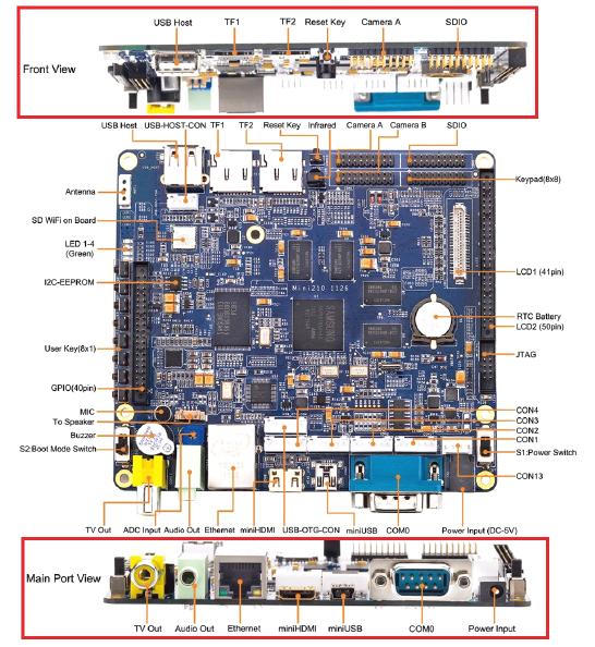
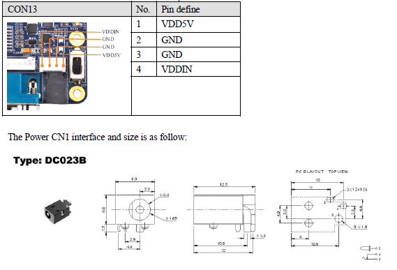
The Mini210 is powered by an external 5V power supply. It has two power inlets: CN1 is for 5V power adapter and the white CON13 is a 4 pin socket used to connect an external power supply when the board is embedded in a closed box.
Serial Port
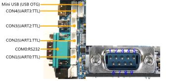
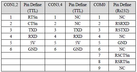
S5PV210 has 4 serial ports: UART0, 1, 2 and 3. UART0 and 1 are 5 wire serial ports and the other two are 3 wire serial ports. On this board, UART0 is converted via RS232 to COM0 and can communicate with a PC via a serial port cable. The rest 4 ports are connected to CPU via CON1-4. They are presented as below:
USB interface
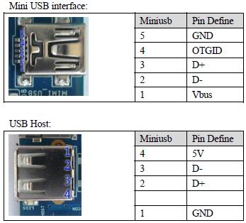
The Mini210 board has two USB interfaces. One is a USB host 2.0 which is the same as a USB interface on a PC and can connect to a USB camera, keyboard, mouse, flash drive and other USB devices. The other is an OTG mini USB 2.0 which is usually used to download programs to a target board. When the board runs Android it can use for ADB debug function.
Network Interface
The Mini210 incorporates a DM9000 chip and can communicate with 10/100M networks. The RJ45 connector includes coupling filters and does not need transformers. With a common network cable,
you can connect a router or switch to the Mini210.
SDWiFi
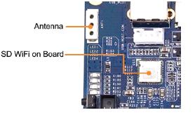
The Mini210 incorporates a SD WiFi Module(Marvell8686 chip) and Antenna on board. Does not need other module, you can use the wifi directorly. The posiont of the SD Wifi module is as follow picture, the datasheet is "WM-G-MR-9-Ref-2.pdf"
Audio Interface
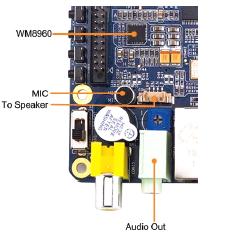
The S5PV210 supports I2S/PCM/AC97. The Mini210 has an I2S0 interface which uses WM8960 as the CODEC chip.The audio output is a 3.5 mm spaced green plug, and WM8960 support D class power amplifier,so mini210 also expand the Speaker socket (CON7), the user can directly connected to 8 Ω 1 W speakers.The input is an on-board microphone. To get better audio quality please move the microphone as close as possible to the audio source when recording.
TV-Out Interface
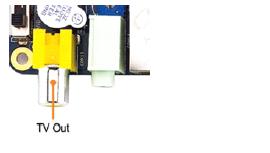
The S5PV210 has one TV output. The Mini210 magnifies the output of DACOUT0, users can connect the board to a TV via an AV cable. Note: when connecting DACOUT0 to a TV users need to switch the TV to the CVBS mode.
HDMI interface
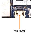
The S5PV210 support HDMI output, the Mini210 expand the HDMI through the Type C miniHDMI interface, users can connect the board to a TV via an HDMI cable. Note: Android support LCD and HDMI output in the same time.
JTAG
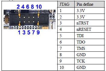
When a board just comes off from production lines it is just a bare board without any data and we usually have to burn the first program to it through the JTAG interface. However since the S5PV210 supports booting from SD card the JTAG is not significant to users any more. Now the JTAG is more often used for debugging. In fact, most of the widely used utilities in markets like JLINK, ULINK and other simulators actually work via the JTAG interface. A standard JTAG has 4 signals :TMS, TCK, TDI and TDO which are test mode select input, test clock, test data input and test data output. These 4 signal lines plus a power line and a ground line form 6 lines in total. In order for testing, most simulators even have a reset signal. Therefore, a standard JTAG is meant to have those signal lines, and it does not mean whether it is 20Pin or 10Pin. As long as a JTAG interface has those signal lines, it will be a standard JTAG interface. The Mini6410 has a 10Pin JTAG interface which has complete standard JTAG signals. Notes: for beginners who just want to focus on Linux or WinCE development, the JTAG interface has no significance because most development boards already have a complete BSP which includes commonly needed serial ports, network port and USB port. When a board runs with Linux or WinCE installed, users can fully utilize more convenient functions and utilities provided by the operating system to debug. They do not need a JTAG. Even if you can trace your programs it will be extremely tough to step debug because it will go into the operating system. This is not an easy job.
LED
A LED is commonly used as a status indicator. The Mini210 has 4 user programmable LEDs which are directly connected to GPIO. The LEDs will be on at a low level voltage. Detailed information is as follows:
User Key
The Mini210 has 8 test keys. They all are CPU interrupt input signals and will be triggered at a low level voltage. They can also be multiplexed to GPIO and other function interfaces. To multiplex them users can extend them through CON12. These 8 keys are defined as follows:
Matrix keyboard
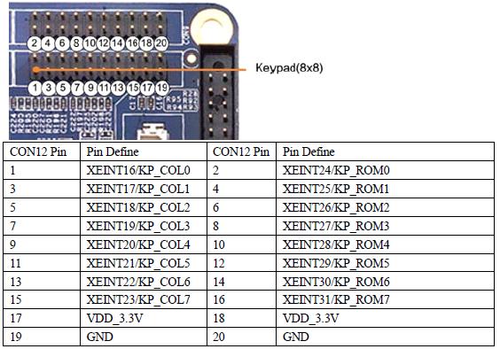
S5PV210 have a 8x8 matrix keyboard, the development board has expended all the keys with CON12 interface, as shown below:
Notice:
- CON12 is the IDC 2.0mm interface, total 20Pin
- XINT16/KP_COL0 said pin change interrupt signal can be multiplexed with XEINT16,
meaning similar to the other pin.
LCD interface
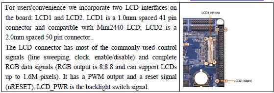
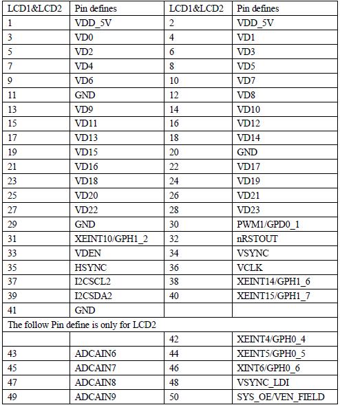
Notice: Because the use of 1-wired touchscreen, LCD1 does not include four-wire resistive touch pin from CPU, but the addition of I2C and interrupt pins (see LCD1-37,, 38,39,40), this is designed to will be able to use capacitive touch screen. LCD2 will include a more extensive CPU pins, or detail table below the schematic.
ADC Input
The Mini210 has 10 A/D conversion channels, According to different purposes, scattered in
various interfaces:
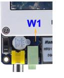
AIN0 is connected to the adjustable resistor W1;
AIN1, 2, 3, 4 and 5 are extended via CON6's 3, 5, 7, 9 and 11 Pins.
AIN 6, 7, 8, 9 was extended via LCD2, it can used for touchsreen.
The S5PV210’s AD conversion can be configured to 10-bit/12-bit.
For users’ convenience, W1 is placed close to one edge of the board and will not be hidden even
when the board is equipped with a 5.0-inch LCD.
PWM Buzzer
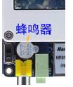
The on-board SPEAKER is controlled by PWM0, the diagram is shown below. PWM0 corresponds to GPD0_0 which can be configured as PWM output via software or used as a GPIO.
Infrared Receiver
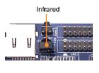
The Mini210 has an infrared receiver. Its type is IRM3638 (or others compatible). It connects to EINT9(GPH1_1).
I2C-EEPROM
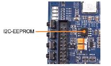
The Mini210 has an EEPROM AT24C08 connected to CPU's I2C. It has 256 bytes memory and is mainly for testing I2C bus.
Micro-SD/TF card
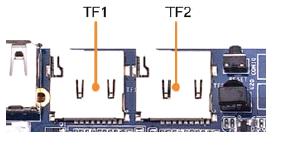
The S5pV210 has four SDIO interfaces.
SDIO0 is commonly used for Micro-SD/TF cards. See the TF1.
SDIO2 is commonly used for Micro-SD/TF cards. See the TF2.
See the follow picture, the interface can support SDHC.
SDIO-II/SD-WiFi interface
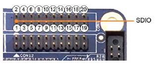
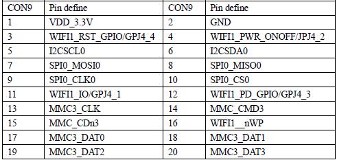
The SDIO4 of the S2PV210 is extended via CON9. It is a 2.0 mm spaced 20 pin connector and
includes an SPI, an I2C and 4 GPIOs.
CMOS camera interface
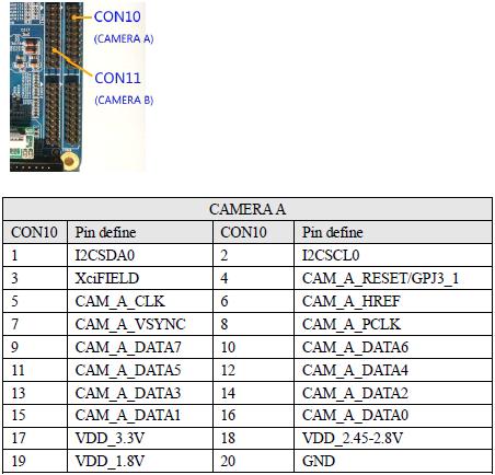
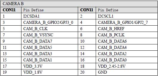
The S3C6410 has two CMOS camera interface. It is extended via CON10(CAMERA A) and
CON11(CAMERA B). It is a 20 pin 2.0mm connector, users can directly use the CAM130 module
we provide. The CAM130 module does not have any circuits. It is basically just a converter and
directly connects to a ZT130G2 camera module.
Notes: the camera interface is a multiplexed port. It can be used as GPIO by setting corresponding registers. The schematic below presents its pin details.
GPIO interface
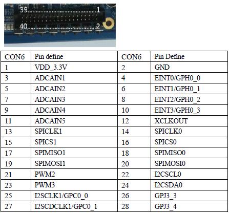
GPIO is the abbreviated form of General Purpose Input Output. The Mini210 has a 40 Pin 2.0mm
spaced GPIO interface, i.e. CON6.
In fact, CON6 has not only quite a few GPIO pins but also some CPU pins such as AD input,
DAC and so on. The SPI interface, I2C interface, interrupts and some others are all GPIOs, but
they are marked as special function interfaces. They can be configured for other purposes too by
setting related CPU registers.
