Difference between revisions of "Micro2440 Introduction"
(→Micro2440 CPU board introduction) |
(→Micro2440 CPU board introduction) |
||
| Line 28: | Line 28: | ||
Specific hardware resource of Micro2440; | Specific hardware resource of Micro2440; | ||
*CPU Processor | *CPU Processor | ||
| − | + | **Samsung S3C2440A, frequency 400 MHz, the highest 533 MHz | |
*SDRAM Memory | *SDRAM Memory | ||
| − | + | **Onboard 64MB SDRAM | |
| − | + | **32bit data bus | |
| − | + | **SDRAM clock frequency up to 100 MHz | |
*FLASH Memory | *FLASH Memory | ||
| − | + | **Onboard 64 MB NAND flash, Power-down non-volatile | |
| − | + | **On-board 2 MB NOR flash, Power-down non-volatile, BIOS has been installed | |
*Interface | *Interface | ||
| − | + | **56-pin 2.0mm GPIO interface PA | |
| − | + | **50-pin 2.0mm LCD&CMOS CAMERA interface PB | |
| − | + | **56-pin 2.0mm system bus interface PC | |
| − | + | **On-board reset circuit | |
| − | + | **On-board 10 Pin 2.0mm JTAG interface | |
| − | + | **4 user debug indicator | |
*System clock | *System clock | ||
| − | + | **12 MHz passive crystal | |
*Power supply | *Power supply | ||
| − | 5V DC | + | **5V DC |
*Dimension | *Dimension | ||
| − | + | **63 x 52mm | |
===CPU board pin description=== | ===CPU board pin description=== | ||
Revision as of 09:23, 5 July 2012
Contents
Micro2440 development board introduction
Note: The hardware resources of Micro2440 is same as the mini2440 in essence, so the software micro 2440 uses is same as mini2440.
The main difference between micro2440 and mini2440 is the interface, micro2440 is motherboard and CPU-board, mini2440 is a integrated board.
Micro2440 development board is constituted of CPU board Micro2440 and mother board micro2440SDK.Mini2440 CPU board is a minimum system development board, it includes the basic system configuration.
- CPU -SUMSUNG S3C2440 operating at 400Mhz
- NOR FLASH- 2M
- NAND FLASH -256M(64M-1G)
- SDRAM -64M (consisted of 2pcs 16 bit 32M SDRAM)
- 1 power indicator and 4 user indicator
- professional reset chip
- professional voltage regulator.
So the user can do the simple test just connecting to the power supply without the motherboard. It is the feature of micro2440 comparing to the other CPU board.
Mini2440SDK based on the mini2440 CPU board is the function-verification motherboard which includes standard RJ-45 network interface, audio input ad output,USB and SD card and etc.
Micro2440 SDK includes the development board tools such as power supply, simple JTAG emulator and other cables.
Micro2440 CPU board introduction
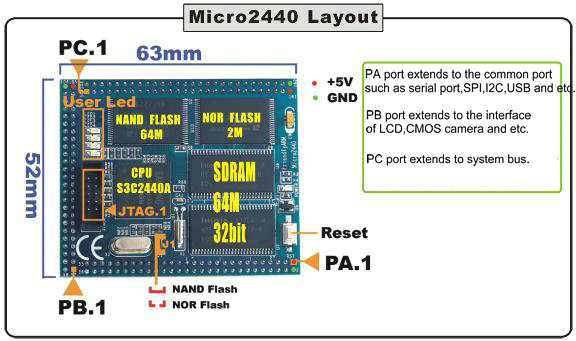
Micro2440 is a minimum system board which includes the basic power circuit(5V),reset circuit, standard JTAG debugger interface, user debug indicator, storage unit and CPU. The flash memory unit includes NAND FLASH and NOR FLASH, system booting from NAND or NOR flash is selected by jumper J1. The Nor flash stores the BIOS.(we store the supervivi), the NAND flash store the complete system program(bootloader, kernel, file system)
Specific hardware resource of Micro2440;
- CPU Processor
- Samsung S3C2440A, frequency 400 MHz, the highest 533 MHz
- SDRAM Memory
- Onboard 64MB SDRAM
- 32bit data bus
- SDRAM clock frequency up to 100 MHz
- FLASH Memory
- Onboard 64 MB NAND flash, Power-down non-volatile
- On-board 2 MB NOR flash, Power-down non-volatile, BIOS has been installed
- Interface
- 56-pin 2.0mm GPIO interface PA
- 50-pin 2.0mm LCD&CMOS CAMERA interface PB
- 56-pin 2.0mm system bus interface PC
- On-board reset circuit
- On-board 10 Pin 2.0mm JTAG interface
- 4 user debug indicator
- System clock
- 12 MHz passive crystal
- Power supply
- 5V DC
- Dimension
- 63 x 52mm
CPU board pin description
The pin description of 3 port on the CPU board is below, you can find it in the schematic.
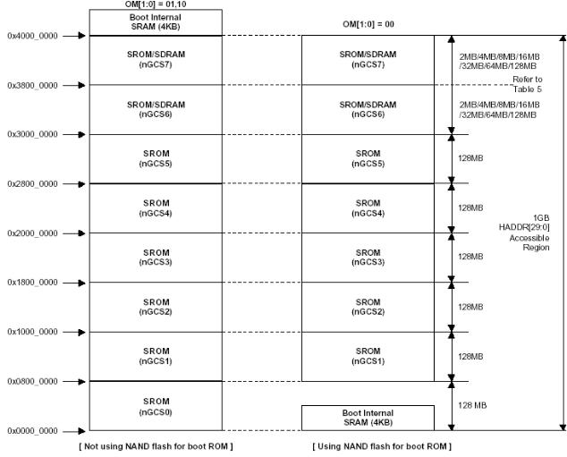
address allocation and chip select signal definition
SC2440 support 2 boot modes : Boot from Nand Flash or from Nor Flash. The allocation of the memories is different in the 2 boot mode.
The allocation of memory in nGCS0 Nor Flash boot mode is on the left side.
The allocation of memory in nGCS0 Nor Flash boot mode is on the right side.
SFR area is the special function register address control.
SRAM storage system
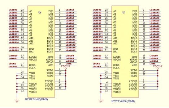
Micro2440 use 2 external 32M bytes 64M bytes SDRAM which is called memory in common, they are connected in parallel to consist of 32-bit bus for increasing the accessing speed. Because they are connected in parallel, so they use nGCS6 as chip select. It decides that their physical initial address is 0x30000000 according to the CPU datasheet 5-2.
Flash storage system
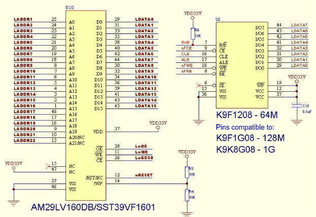
Micro2440 is equipped with 2 types Flash, one is NOR FlashSST39VF1601(AMD29LV160DB is compatible with this pin), another is NAND Flash whose type is K9F2G08, size is 256M(up to 1G Nand Flash). S3C2440 support two types flash to boot system. You can select to boot from NOR Flash or Nand Flash via toggling the switch S2. Actually the one NAND flash is enough in ARM product. But we preserve the NOR flash for user's learning.
NAND Flash doesn't have the address bus, it has special control interface connecting to CPU, the data bus is 8-bit, but it doesn't mean that the rate of accessing data is slow. Most of the USB flash disk and the SD card is made of NAND Flash.
Nor Flash uses A1-A22, 22 address lines in all and 16 data lines connected to CPU according to the schematic below. Please note that the address start from A1, it means that the minimum unit of reading and writing is 2-bytes.So according to the schematic, it is designed for up to 8M bytes Nor Flash. Actually we have used address lines A1-A20, because the pins of SST39V1601 connected to A21 and A21 is NC.
Power circuit
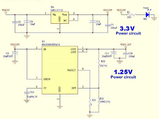
The development board use external 5V power supply which produces the the 3.3V and 1.25V the system needed via the voltage regulator.
Reset circuit
Micro2440 includes built-in reset circuit, it use reset chip MAX811 to achieve the low level reset.
User LED
Micro2440 has 4 user-programmable LED connected to GPIO of CPU, active low.
JTAG
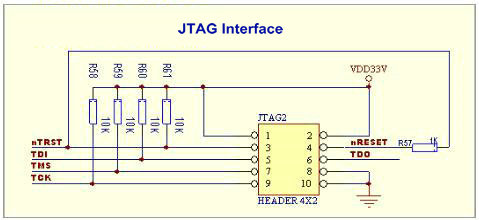
Micro2440 has a standard 10-pin JTAG interface which includes standard JTAG signal. The pin definition is below.
Micro2440SDK motherboard
=Micro2440SDK motherboard layout and instruction
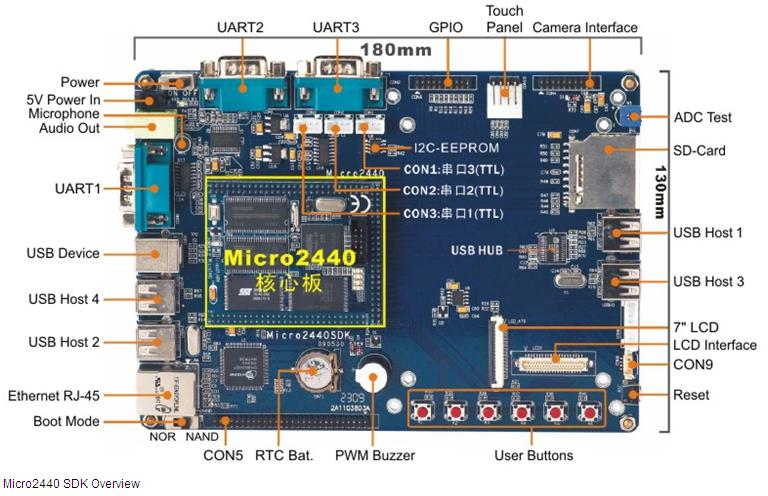
Micro2440sdk motherboard's layout and interface is below, it's a 2-layer PCB and draw out the common interface situated in the one side of the board. The other I/O and system bus are break out to the 2.0mm pitch headers
Micro2440SDK motherboard features;
- Dimension:180 x 130 mm
- EEPROM:1024 Byte (I2C)
- Ext. Memory:SD-Card socket
- Serial Ports:3x DB9 connector (RS232)
- USB:4x USB-A Host 1.1, 1x USB-B Device 1.1
- Audio Output:3.5 mm stereo jack
- Audio Input:3.5mm jack (mono) + Condenser microphone
- Ethernet:RJ-45 10/100M (DM9000)
- RTC:Real Time Clock with battery (CR1220)
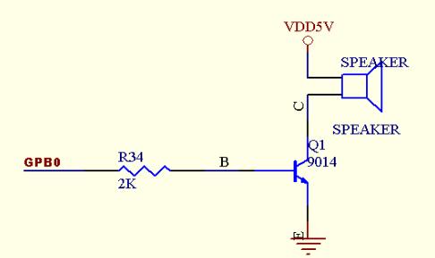
- Beeper:PWM buzzer
- Camera:20 pin Camera interface (2.0 mm)
- LCD:41 pin connector for FriendlyARM Displays and VGA Board
- Touch Panel:4 pin (resistive)
- User Inputs:6x push buttons and 1x A/D pot
- Expansion headers(2.0 mm)
- Power:regulated 5V (DC-Plug: 1.35mm inner x 3.5mm outer diameter)
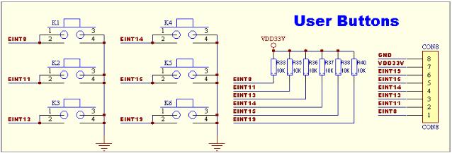
User's button
Mini2440SDK has 6 user testing buttons leading to the CPU interrupt pins (active-low) and these pins can be used as GPIO and special function interface for users. And the 6 pins is also lead to CON8.
AD input test
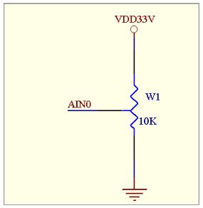
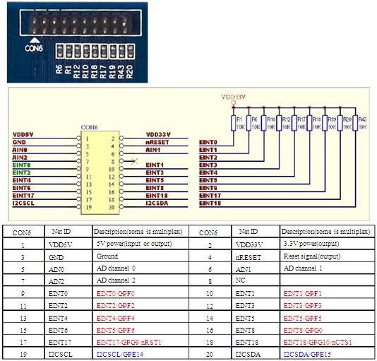
Mini2440SDK motherboard has 3 channels A/D which located in CON6. The AIN0 is linked to variable resistor W1.
PWM buzzer
The speaker is controlled by PWM, GPB0 can be used as PWM output by software.
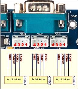
Serial port
S3C2440 has 3 serial port UART0、1、2, UART0,1 can constitute of a full-function serial port. In most applications, we just use the three simple serial port relating to CON1、CON2、CON3. For the users convenience, the UART0、1、2 is converted to RS232 corresponding to COM0、COM1、COM3.
USB interface
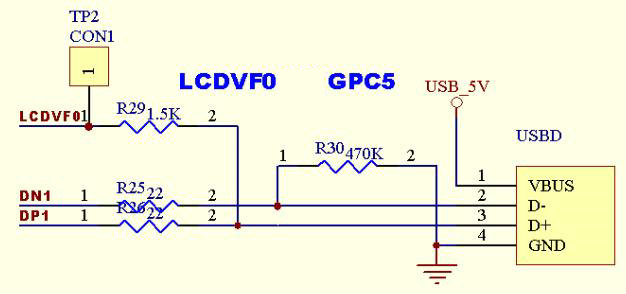
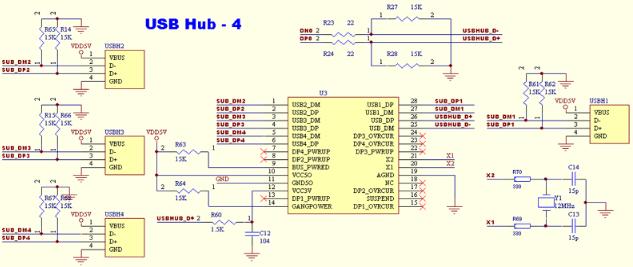
Micro2440SDK mother board has 2 USB, one is USB host which can be expanded to 4 USB Host which could connected to USB camera, USB key board and etc via USB hub. Another one is USB slave which is usually used to download programs to a target board. When the board runs WinCE it can synchronize with a Windows via ActiveSync. For Linux there are no programs for synchronization for now. USB slave schematic is below:
USB hub schematic is below:
LCD interface
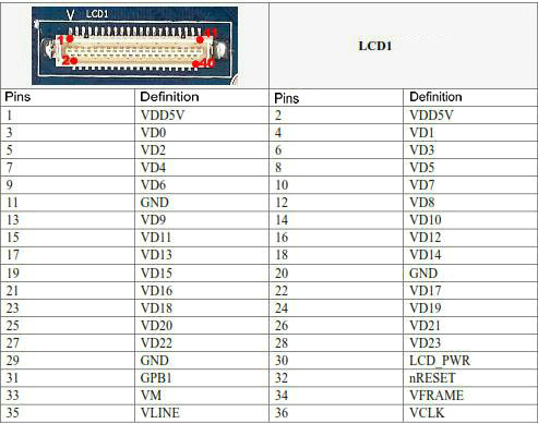
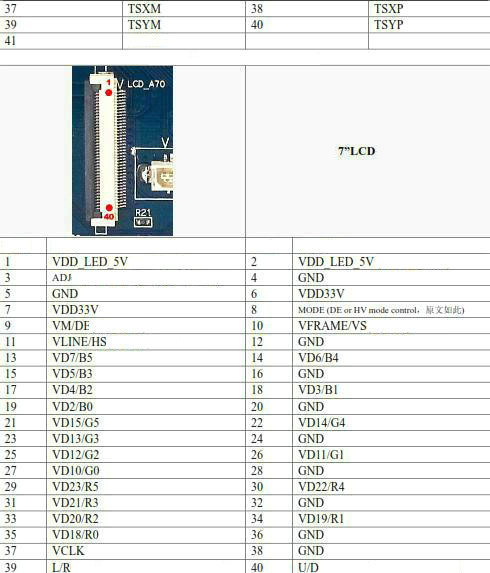
Micro2440 has 2 LCD interface: LCD1 and LCD_A70, most of the data signals leading to CPUof them is same virtually.
LCD1 interface is a 41pin 0.5mm white mount which is same as mini2440, including the most control signals and RGB outputs of the common LCD, we also draw out the PWM output and nRESET signals. In addition, 37、38、39、40 is 4-wire touch screen interface.
LCD_A70 is for Innolux 7”LCD.
EEPROM
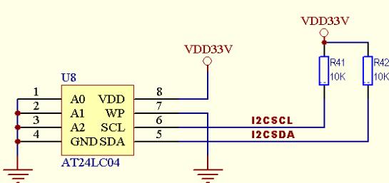
Micro2440 has a 256K bytes EEPROM ATC24C08 connected to I2C pin of the CPU for user testing I2C.
Network interface
Micro2440 incorporates a DM9000 chip and can communicate with 10/100M networks. The RJ45 connector includes coupling filters and does not need transformers. With a common network cable, you can connect a router or switch to the Micro2440.
Audio interface
S3C2440 includes built-in I2S bus directly connected to external 8/16 bit stereo CODEC. Micro2440 uses UDA1341 chip based on I2S to achieve the audio decoder system. The initialization and settings of the internal registers of UDA1341 is achieved by L3-bus, here we use the Samsung public domain designation in which GPB2、GPB3、GPB4 of CPU simulate L3MODE、L3DATA、L3CLOCK signal specified by L3-BUS.They are unused after initialization.
GPIO
Most pins of PA port on the CPU board can be used as GPIO, but most of them has its own specific function such as serial port, I2C , USB and etc,we can identify them in the schematic. With the pins unused and the pins not for special function, they are break to CON6 also including pins not GPIO. So we name CON6 as GPIO generally.
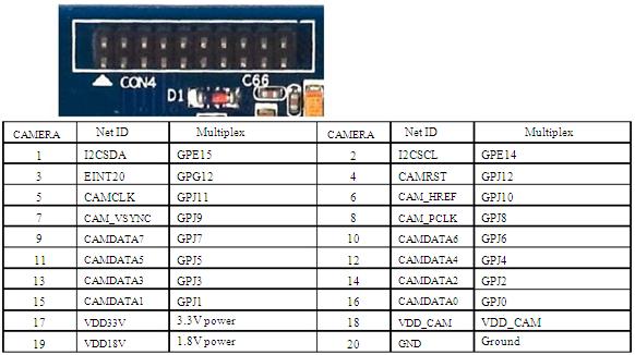
CMOS camera interface
The Micro2440 has a CMOS camera interface. It is extended via CON4. It is a 20 pin 2.0mm connector, users can directly use the CAM130 module we provide. The CAM130 module does not have any circuits. It is basically just a converter and directly connects to a ZT130G2 camera module.
Notes: the camera interface is a multiplexed port. It can be used as GPIO by setting corresponding registers. The schematic below presents its pin details.
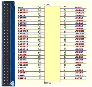
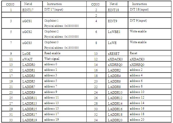
System bus interface
Mini2440’s system bus interface is CON5 including 16 dataline(D0-D15), 25 address line(A0-A24) and other control singal line(CS, RESET,W/R), CON5 can provide 5V voltage. Actually few user expands peripherals via bus.
