Difference between revisions of "CY7C68013"
(→resource) |
(→where to get) |
||
| (One intermediate revision by the same user not shown) | |||
| Line 147: | Line 147: | ||
[[Media:CY7C68013A 14A 15A 16A 38-08032.pdf]] | [[Media:CY7C68013A 14A 15A 16A 38-08032.pdf]] | ||
| + | |||
| + | |||
| + | |||
| + | ==where to get== | ||
| + | |||
| + | [http://www.geeetech.com/cypress-cy7c68013a-ezusb-fx2lp-usb20-development-boardmodule-p-634.html here] you can get one. | ||
Latest revision as of 03:25, 28 August 2014
Contents
introduction
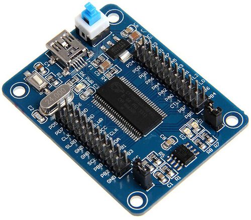
CY7C68013A is a development board, with CY7C68013A-56PVXC microcontroller as the main control chip which is an enhanced revision of 8501 integrated chip; it has an integrated IIC controller. In addition, it is perfectly functionally compatible with USB2.0_USB_IF communication by connecting with USB cable. (Read more in CY7C68013A-56PVXC data book.
This development board can provide power supply and establish communication connection with USB cable, the stabilivolt AMS1117 provides 3.3v for master control, all the pins of CY7C68013A-56PVXC are broken out to be connectors, making it easy for the connection of peripheral circuit and with other modules; for the measuring and testing of pins. Furthermore, AT24C128 chip and relevant circuit are designed for this development board, program can be uploaded into AT24C128 through USB, and you can read and write by controlling the jumper cap (plug in the jumper cap, AT24C128 closed, pull it off, AT24C128 opened),which effectively make up for the lack of ROM storage in CY7C68013A-56PVXC,making it a more perfect CY7C68013A-56PVXC learning board.
Overview and Hardware Resources
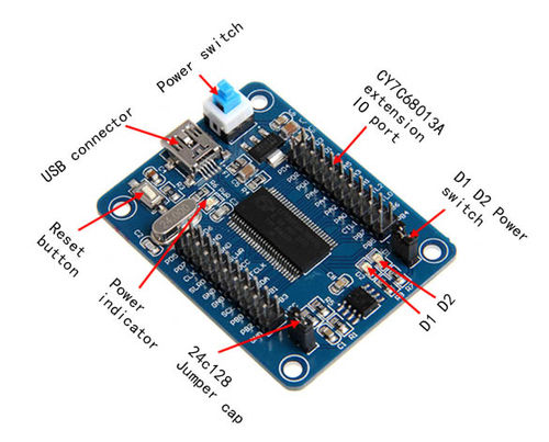
1.A USB interface
2.A bunch of extension port
3.A power indicator
4.A jumper that controls the open and close of data memory read and write of AT24C128
5.A power switch
6.A reset button
7.Weight: 14g
8.Size: 55mm*42mm*10mm
Interfaces
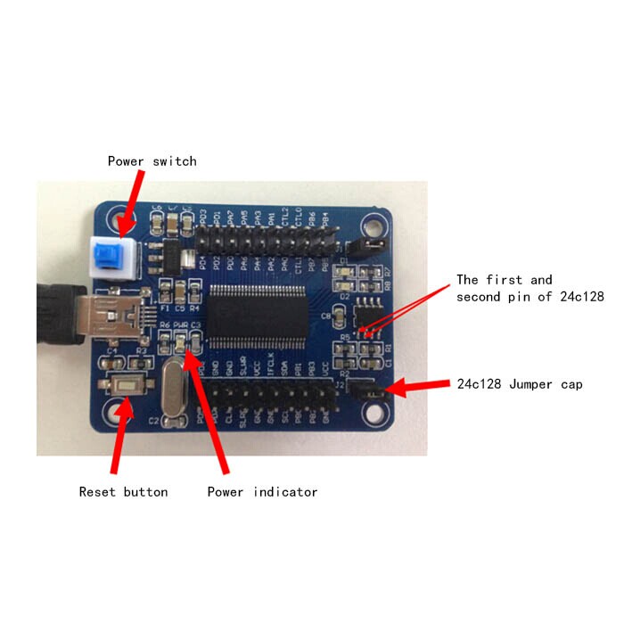
Interface Layout
Interface specifications
USB interface: For circuit board power supply and the uploading program for CY7C68013A. Extension IO port: all the pins of CY7C68013A are broken out as connectors in the form of header, Power switch: for the open and close of power supply to the PCB through USB interface Reset button: reset the main
Jumper Instruction
Jumper cap of 24C128: controlling the ability of data reading and writing. Plug in the cap, AT24C128 is closed; remove it, AT24C128 is started.
Jumper cap of D1, D2: controlling the power of LED light. Plug in the cap, the anode of LED 1 and 2 will be connected to the positive pole of power source through resistance. Remove the cap, the anode of D1 and D2 will be open.
Development Environment setting
Interface Connecting and Setting
Connect the CY7C68013A to computer with a USB cable when performing functional test for it.
Get Started
Program uploading and testing of CY7C68013A RAM
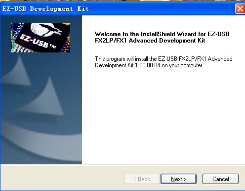
Open the folder of CY7C68013A development board, find development tools fx2lp.exe( the following picture), install the uploading program soft, choose next or yes until finish.
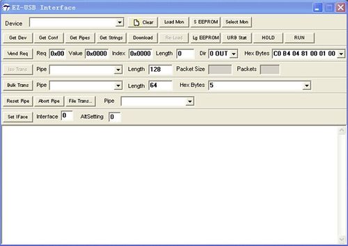
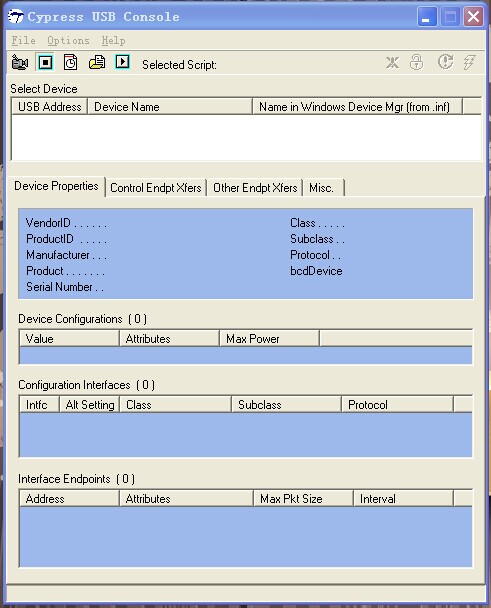
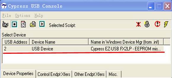
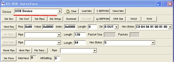
1.Click start> all programs>cypress> CyConsole EZ-USB, open the uploading software, (picture below), the can see the following interface
2 Connect CY7C68013A to PC with a USB cable
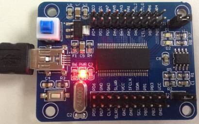
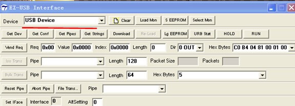
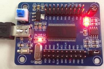
3 Press the power switch, the PWR on the board will light, USB Device will appear in the device field of EZ-USB Interface and the field of select device in Cypress USB Console will respond correspondingly, indicating the connection with USB.
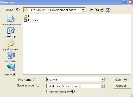
4 Click Download button in EZ-USB Interface, open the CY7C68013A development board folder, double click the liu.hex file, then you can began uploading.
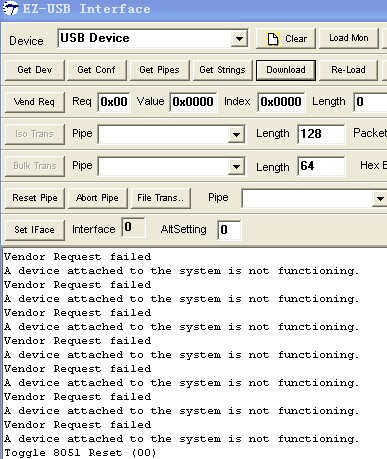
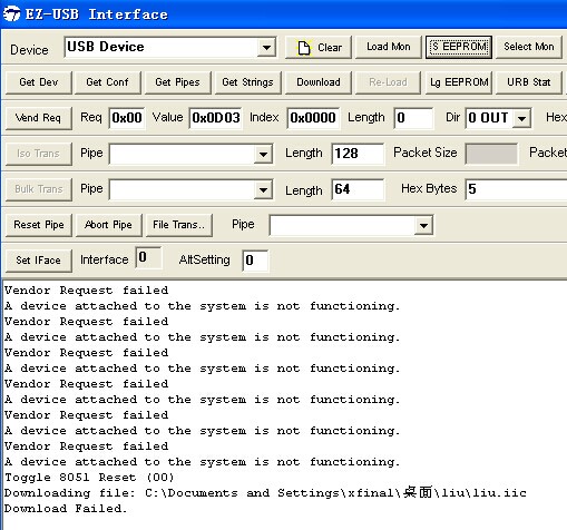
5 If the EZ-USB Interface displays as the following interface, the program uploading failed.
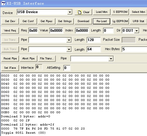
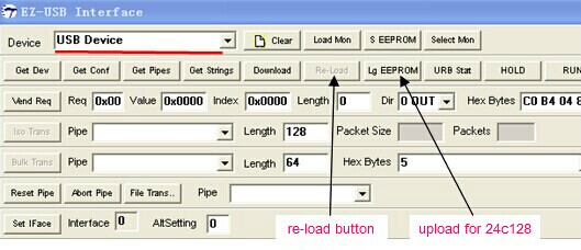
6 Press the reset button on the board, the device field in EZ-USB Interface will be blank, release the button, USB Device appears, then click re-load to upload program again. The following interface indicates the success of uploading.
7 At this moment, the LED (D1 and D20 will blink, indicating everything goes well with the IC and the circuit.
NOTE: the program uploaded for ARM will purge automatically after power off.
Program uploading and testing for AT24C128
- Remove the 24C128 jumper cap on the board (start data memory read and write function of AT24C128)
- Follow the steps of 1-4 in CY7C68013A RAM program uploading.
- Break the circuit of the first and second pin of AT24C128, press the power button, the power indicator (PWR) is on, the Device field in EZ-USB Interface will show USB Device, the Select Device in Cypress USB Console will give response, too, indicating USB is connected.
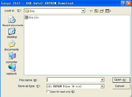
(4)Click S EEPRROM button in EZ-USB Interface, open CY7C68013A folder, double click liu.iic file to upload program.
(5)The following interface in EZ-USB Interface shows program upload failed.
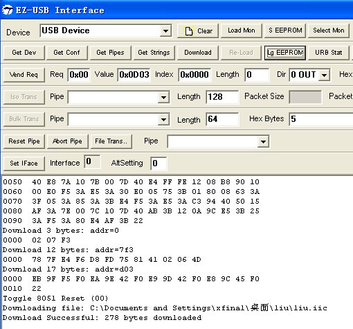
(6)Press the reset button on CY7C68013A, the Device field in EZ-USB Interface will show blank. Release the reset button, USB Device appears again. Release the short-cut of pin 1 and 2 of AT24C128, click Lg EEPROM button, then double click liu.iic file to upload. The following interface shows the uploading succeeds.
(7)Reboot CY7C68013A, LED D1 and D2 will blink, indicating everything works well. Note: the program uploaded in AT24C128 will not be cleaned up automatically after de-energized.
FAQS
(1)Program uploading failed for CY7C68013A RAM. a)Make sure you pressed the power button on the board and the jumper cap on 24C128 has been plugged in (close data memory read and write function of AT24C12). b)If the Device field in EZ-USB Interface shows USB Device and the Select Device in Cypress USB Console gives response after you connected the USB and pressed the power button, otherwise, you should check the connection.
c)Note: press the reset button before uploading until the following interface appears, click re-load button.
(2)program uploading failed for 24C128
a)Remove the jumper cap of 24C128 (start data memory read and write function of AT24C12) before uploading.
b)Note that pin 1 and 2 should be short-cut before energizing, press reset button before uploading program, release the short-cut of pin 1 and 2 right after you release the reset button and the interface appears.(4-15). Click Lg EEPROM, double click liu.iic file, program uploading begins.
(3)D1, D2 are not able to operate.
Check if the jumper cap of D1 and D2 are plugged and well connected (jumper cap on D1 and D2 is the controller of LED. As in intrfaces layout.
resource
PC software:SDK new version fx2lp. exe
test code file:liu.hex、liu.iic
Media:CY7C68013Adevelopment board.rar
data sheet
Media:CY7C68013A 14A 15A 16A 38-08032.pdf
where to get
here you can get one.
