Difference between revisions of "EP2C5T144C8"
From Geeetech Wiki
(→I/O Configuration) |
(→Download Mode) |
||
| (14 intermediate revisions by the same user not shown) | |||
| Line 2: | Line 2: | ||
== Introduction == | == Introduction == | ||
| − | [[File: | + | [[File:ENC1.jpg | 450px]] |
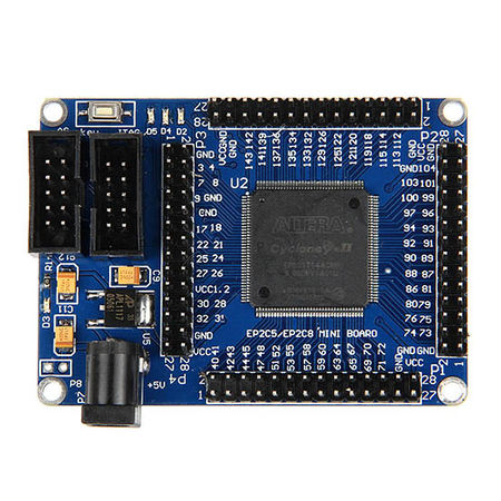
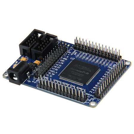
The board adopts CycloneIIEP2C5T144 chip of ALERA company as the core,users can easily use the FPGA chip embedded in actual system.The board can complete simple logic control,data acquisition,signal processing,math,etc.The board also support the NiosII embedded development.All the I/O port and the chip clock pin through the row needles to elicit,these interfaces can be extended any memory and peripherals. | The board adopts CycloneIIEP2C5T144 chip of ALERA company as the core,users can easily use the FPGA chip embedded in actual system.The board can complete simple logic control,data acquisition,signal processing,math,etc.The board also support the NiosII embedded development.All the I/O port and the chip clock pin through the row needles to elicit,these interfaces can be extended any memory and peripherals. | ||
| Line 9: | Line 9: | ||
== I/O Configuration == | == I/O Configuration == | ||
'''1'''、50MHz crystals; | '''1'''、50MHz crystals; | ||
| − | <br> | + | <br>'''2'''、LED D2 - Pin3; |
| − | <br> | + | <br>'''3'''、LED D4 - Pin7; |
| − | <br> | + | <br>'''4'''、LED D5 - Pin9; |
| − | <br> | + | <br>'''5'''、Key - Pin144; |
== Download Mode == | == Download Mode == | ||
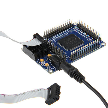
| + | '''AS Mode''' | ||
| + | <br>[[file:ENC3.jpg | 450px]] | ||
| + | <br>'''Jtag Mode''' | ||
| + | <br>[[file:ENC4.jpg | 450px]] | ||
== Resources == | == Resources == | ||
| Line 21: | Line 25: | ||
| − | == | + | ==How to buy == |
| + | |||
| + | Click here to buy [http://www.geeetech.com/altera-cycloneii-ep2c5t144-fpga-dev-board-p-262.html Altera CycloneII EP2C5T144C8 FPGA Dev Board] | ||
Latest revision as of 11:34, 22 May 2014
Introduction
The board adopts CycloneIIEP2C5T144 chip of ALERA company as the core,users can easily use the FPGA chip embedded in actual system.The board can complete simple logic control,data acquisition,signal processing,math,etc.The board also support the NiosII embedded development.All the I/O port and the chip clock pin through the row needles to elicit,these interfaces can be extended any memory and peripherals.
I/O Configuration
1、50MHz crystals;
2、LED D2 - Pin3;
3、LED D4 - Pin7;
4、LED D5 - Pin9;
5、Key - Pin144;
Download Mode
Resources
How to buy
Click here to buy Altera CycloneII EP2C5T144C8 FPGA Dev Board


